
The Complete Guide to Plasma Treatment for Electronics
Plasma surface treatment is one of the most utilized manufacturing processes in the electronics industry. Learn everything you need to know about plasma treatment and electronics in our complete guide below.
What Is Plasma Treatment?
Before we get into plasma treatment and its use in electronics and other industries, we must explain what plasma surface treatment means and how it works. Plasma treatment, in simple terms, is a process for activating the surface substrate of a material. This process alters the surface of a material that typically has a low-wettability surface, like plastic, which means that it doesn’t bond with liquids like glue, paint, ink, or other coatings.
Anyone who’s tried to paint a plastic surface can understand that plastic is generally incompatible with coatings. But plasma surface treatment activates the surface of the plastic so that these liquids and coatings adhere much better. With plasma surface activation, gluing parts with low-wettability surfaces like plastic together is much easier and more reliable.
What Is Plasma Cleaning?
The other result of plasma treatment is surface cleaning. Not only does the plasma treatment activate the surface of a substrate, but it also cleans it of any contaminants that could interfere with the bonding to create a pristine surface.
Again, anyone who’s had to glue or paint something before knows it’s better to do so with a clean surface, so cleaning it first is necessary. Plasma treatment does this all at once by cleaning the surface and activating the substrate.
How Plasma Surface Treatment Works
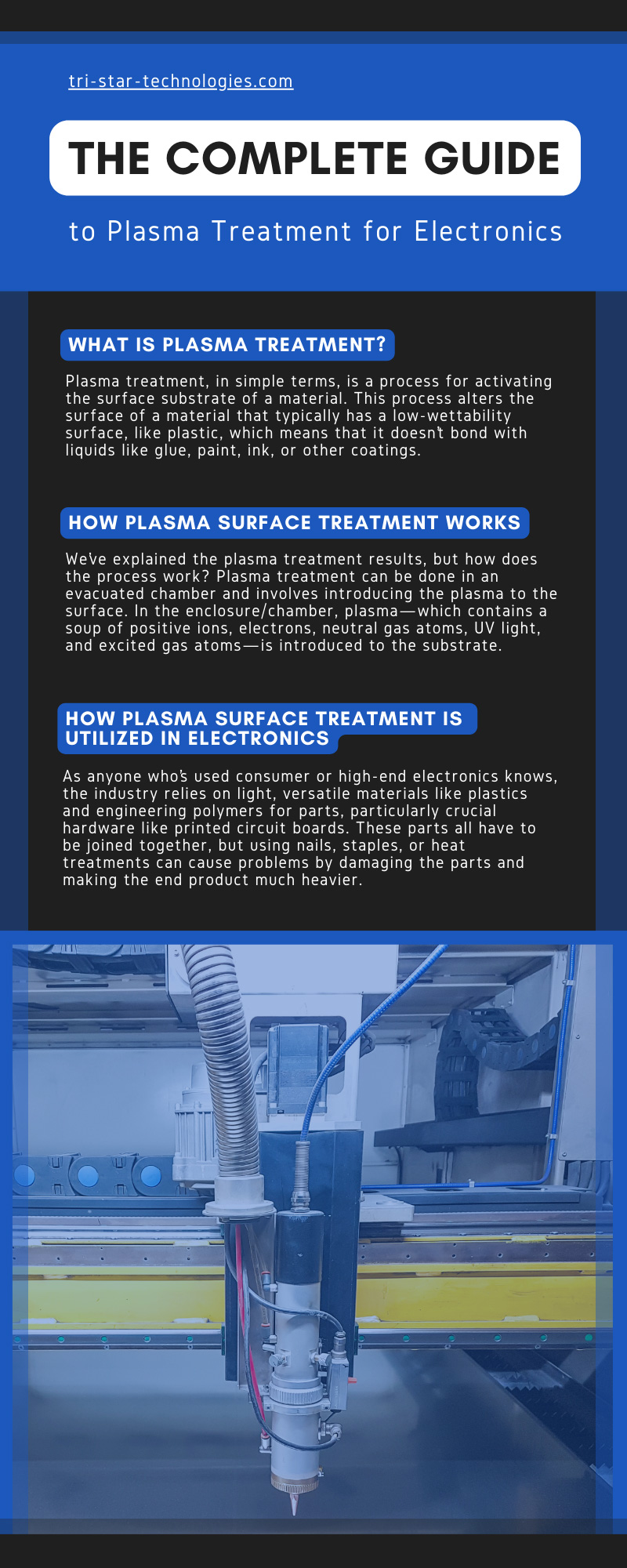
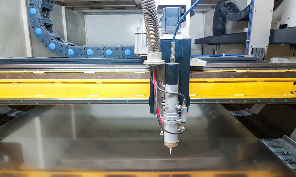
We’ve explained the plasma treatment results, but how does the process work? Plasma treatment can be done in an evacuated chamber and involves introducing the plasma to the surface. In the enclosure/chamber, plasma—which contains a soup of positive ions, electrons, neutral gas atoms, UV light, and excited gas atoms—is introduced to the substrate.
The UV light in the plasma breaks down the organic bonds of the contaminants on the surface to clean the substrate of things like oil and grease. The energetic oxygen species in the plasma reacts with contaminants to form water and carbon dioxide, which is pumped away from the process. The active oxygen species also binds to the surface to activate the substrate of the material and make it highly active to bonding agents and other coatings like paint or ink.
How Plasma Surface Treatment Is Utilized in Electronics
Now we understand how plasma surface cleaning and activation works, but how is it useful for electronics? As anyone who’s used consumer or high-end electronics knows, the industry relies on light, versatile materials like plastics and engineering polymers for parts, particularly crucial hardware like printed circuit boards.
These parts all have to be joined together, but using nails, staples, or heat treatments can cause problems by damaging the parts and making the end product much heavier. This presents a conundrum for the industry—how do we keep our sensitive, plastic parts with low-wettability surfaces together without damaging them? The answer is plasma surface treatment to make these sensitive parts more attractive to bonding agents.
Other Common Applications for Plasma Surface Treatment
While plasma activation and cleaning are commonly employed in the electronics industry, it’s far from the only industry that uses the treatment process. The aerospace industry is one of the biggest users of the process, as it allows for the bonding of lightweight and durable aircraft materials without using chemicals or tools.
The automotive industry utilizes plasma treatment for the same reason—to bond parts together while keeping the product light and cleaning parts thoroughly. In the medical industry, plasma treatment is a common process in equipment manufacturing and assembling small parts like syringes and fine-cleaning medical implants before surgery.
The Benefits of Plasma Treatment for Electronics
We’ve explained plasma treatment and how it works in this complete guide, but what advantages does it offer for electronics over other processes?
Parts Reliability
The plasma treatment process’s main advantage for electronics is that it ensures greater parts reliability for manufacturers. With plasma surface cleaning and activation, parts can be more reliably bonded to one another for more sturdy and durable products.
It also means that ink, paint, and whatever coatings are applied to the surface of electronic parts will bond better and faster for a more thorough coating.
Material Versatility
Another great benefit of the plasma treatment process is its versatility and usefulness for various materials. Plasma surface is useful to practically any material that typically has a low-wettability surface, including:
- Plastics (polypropylene, polyethylene)
- Composites
- Polymers
- Glass
- Metals and alloys
- Ceramics
This versatility means manufacturers don’t have to worry about using a different surface treatment process for every different material. Plasma treatment can get the job done, no matter what surface needs to be cleaned or activated.
Eco-Friendly Process
Plasma surface treatment is also one of the most environmentally friendly processes available. Traditional surface treatment processes that were common before plasma relied either on high temperatures or harmful chemicals to change the surface of a substrate.
Either process would require an incredible amount of energy or harmful chemicals that must be disposed of. Plasma treatment, on the other hand, is a low-temperature process, so it requires little energy and doesn’t produce any harmful waste. It’s the most eco-friendly and cost-effective process.
Cost-Effective
Plasma treatment is also favored because it’s affordable and incredibly cost-effective. As mentioned, plasma treatment doesn’t require heat or chemicals—only readily available gases like oxygen and inert gases.
Outside of the initial investment and startup costs, plasma treatment is the most affordable and cost-effective option, making it incredibly attractive to the electronics and other industries.
Non-Damaging
As mentioned, the electronics industry also favors plasma treatment because it’s a non-damaging process. We all know that electronics require sensitive materials that could break or degrade from harsh treatment from chemicals or temperatures.
As we know, plasma treatment doesn’t require chemicals or heat and is much more sensitive to the surface substrate, cleaning and activating the surface without damaging its structural integrity.
Where To Get Plasma Treatment Systems
If your industrial process could benefit from a plasma treatment system, Tri-Star Technologies can help. Browse our products online, which range from plasma treatment systems to automatic crimping machines and more. Contact our helpful staff if you have any questions about plasma treatment or want to learn more.